PCB Footprint & Dimensions
The recommended module footprint is shown in the xPico 200 Dimensions SMT Module image. The antenna region should ideally be placed on the edge of the board. The antenna location inside of the end unit and installation should be chosen such that the antenna has as clear as possible line of sight to the connecting WLAN devices. The antenna path should be as clear as possible from metal, ground and power planes from adjacent PCBs and other objects that can interfere with the signal path to the connecting WLAN devices.
Access CAD Files
The Platform PCB Package containing all artwork and CAD files can be downloaded at the Lantronix xPico 240 product page and the Lantronix xPico 250 product page.
Platform PCB Package Contents
- xPico 200 reference board CAD package contents
- Reference board pdf and STEP mechanical drawings
- xPico 200 module pdf and STEP mechanical drawings
- Reference board pdf and Orcad schematics
- Reference board bill of materials
- Reference board Mentor PADS artwork and gerber files
- xPico 200 module Mentor PADS symbol
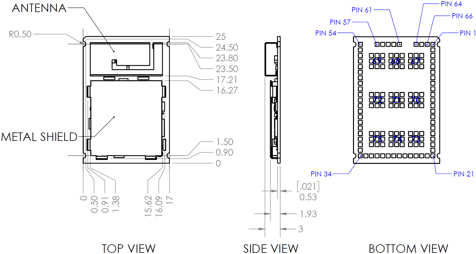
xPico 200 Dimensions SMT Module
SMT Gateway with Dual U.FL Wi-Fi Antenna
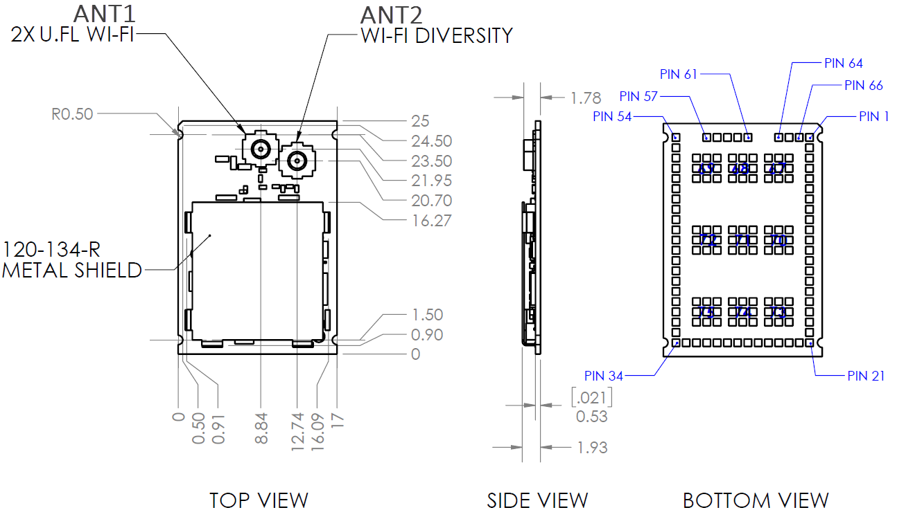
Note
Wi-Fi diversity is not available on units with Bluetooth.
SMT Gateway with On-Module Antenna
xPico 200 Dimensions Edge Connector Module
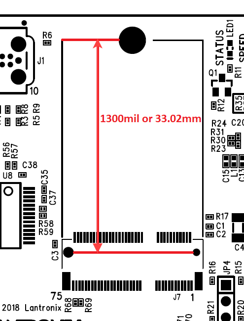
The edge connector module mates to TE connectivity part number 2199230-4.
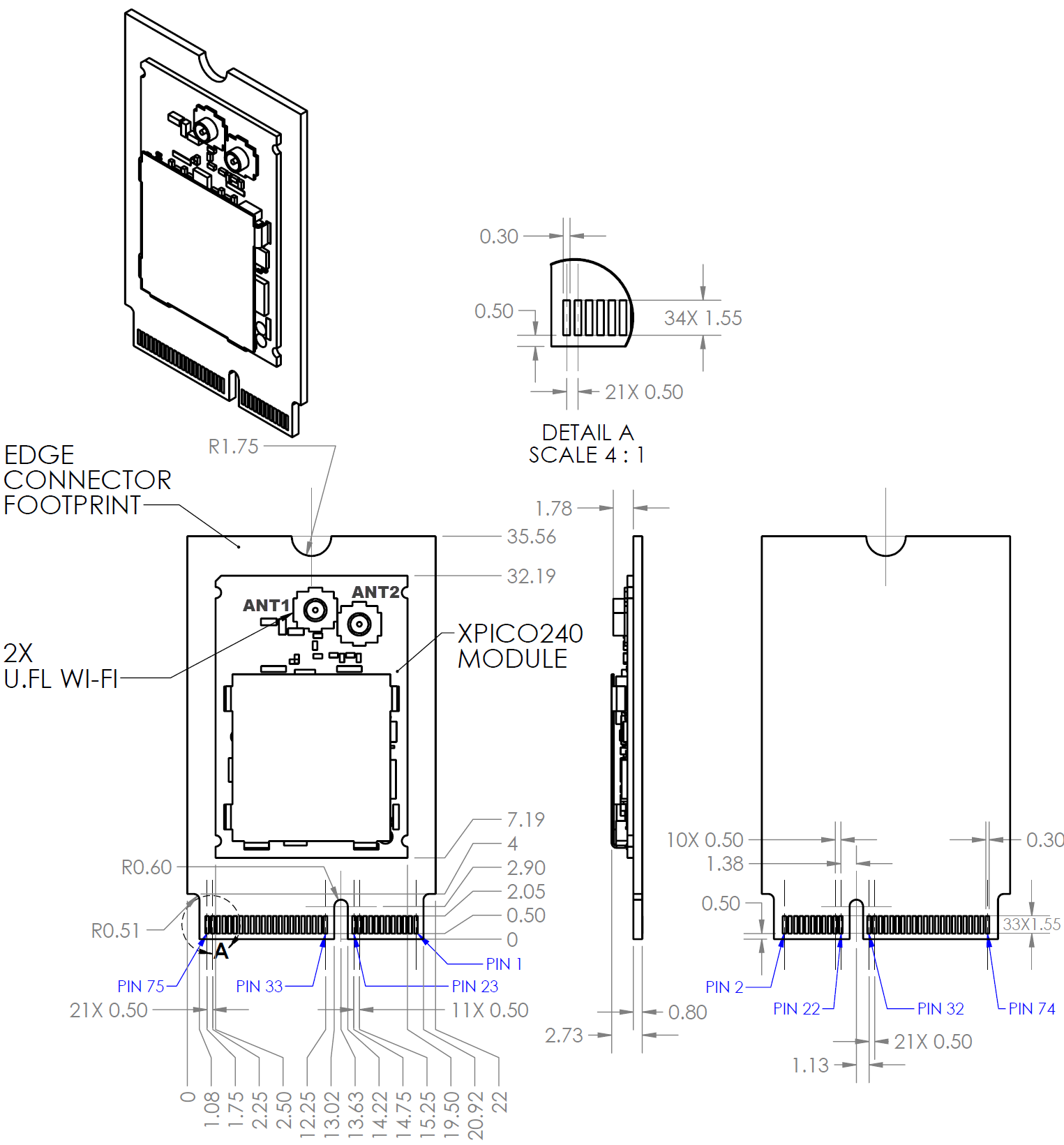
The center-to-center distance from the large mounting hole to the two mounting peg holes for the M.2 connector measures 1300 mil or 33.02 mm.
xPico 200 Recommended Footprint (SMT Module)
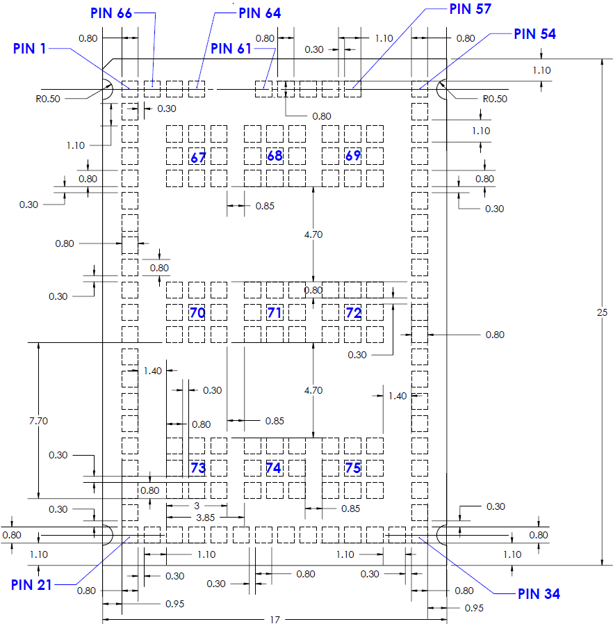
Footprint and artwork files are available for Mentor PADs. These files are included in the Platform PCB Package which can be downloaded at the Lantronix xPico 240 product page and the Lantronix xPico 250 product page.
Lantronix recommends using a minimum of a four layer circuit board for better emission and noise performance. The evaluation kit edge module included in the platform reference package artwork has six layers.
Lantronix recommends using non-solder-mask defined (NSMD) pads for the outer signal pads. The large ground pads are solder mask defined (SMD) into an array of 3x3 individual solder mask openings. Lantronix recommends using ENIG finish for the xPico 200 gateway pads.
The internal ground pads are used for module signal ground and thermal relief. The outer layers should be flooded with ground and the ground pads should have many vias to the internal ground layers. We recommend a ground pad via in each of the solder mask openings on the nine different 3x3 ground pads. The ground pad vias should be via-in-pad directly to the ground plane. The ground pad via-in-pad should also be filled to prevent solder wicking into the via.
Soldering coverage should be maximized and checked via x-ray for proper design. There is a trade-off between providing enough soldering for conductivity and applying too much, which allows the module to “float” on the pads creating reliability issues. Lantronix recommends 80% or more full contact solder coverage on each of the internal ground pads after reflow.
Reflow Profile Guideline
The reflow profile is dependent on many factors including flux selection, solder composition, and the capability of the user's reflow equipment.
Lantronix does not recommend a specific reflow profile but provides the following general guidelines:
- For the SMT modules, Lantronix recommends a maximum of 3 (three) reflow cycles.
- The solder composition typically sets the peak temperatures of the profile.
- Lantronix recommends lead free solder pastes SAC305: Type 4. Water soluble or no-clean solder pastes are acceptable.
- Do not wash the xPico 200 module.
- Reflow equipment is needed at nine heater zones at minimum. Lantronix recommends a forced air type reflow oven with nitrogen.
- Lantronix recommends that the peak temperature at the solder joint be within 237°C ~ 250°C, and the maximum component temperature should not exceed 260°C.
- Lantronix recommends that the solder joint heating time above 217°C last between 30-90 seconds, and at a minimum of 30 seconds.
- Excessive ramp/cooling rates (>3° C/s) should be avoided.
- To develop the reflow profile, Lantronix recommends that the user place thermocouples at various locations on the assembly to confirm that all locations meet the profile requirements. The critical locations are the gateway solder joints.
- When developing the reflow profile, Lantronix recommends that a fully loaded assembly be used to assure that the total thermal mass is accounted for.
Recommended Reflow Profile
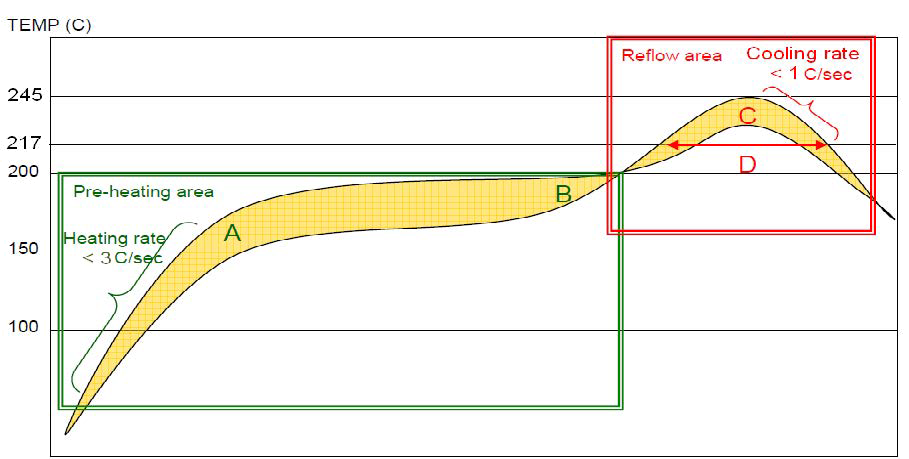
- Solder paste alloy: SAC305(Sn96.5/Ag3.0/Cu0.5)(Lead free solder paste is recommended by Lantronix.)
- A-B. Temp.(Pre-heat): 150~200 °C; soak time: 60~120 seconds.
- C. Peak temp: <250 °C
- D. Time above 217 °C: 30~90 seconds
- Suggested optimal cooling rate is <1 °C /sec. from peak to 217 °C.
- Utilize a minimum of nine heater zones for Reflow equipment.
- Nitrogen usage is recommended when the oxygen concentration is controlled at less than 1500 ppm.
- Inspect solder joint by X-ray post reflow for voiding and solder shorts.
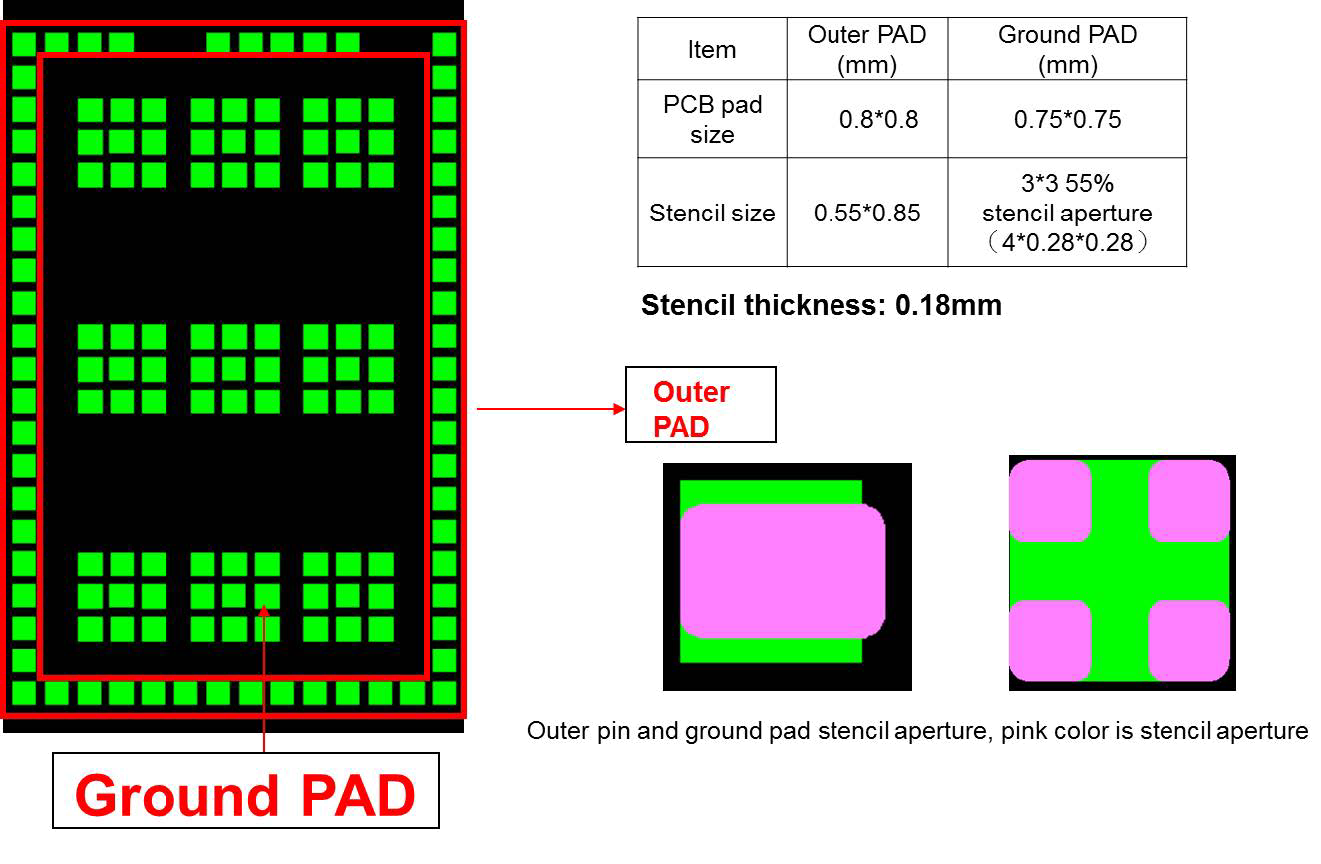
Stencil Recommendations
Sample Solder Process Using 0.18 mm Stencil
MSD (Moisture Sensitive Device) Control for the Module
- The xPico 200 gateway is a moisture sensitive device; the MSL level is 3.
- Modules to be subjected to reflow solder or other high temperature processes must be mounted within 168 hours of opening the vacuum containment bag in factory conditions.
- The module requires baking before mounting, if:
- the Humidity Indicator Card reads >10% when read at 23± 5°C
- or the MSL3 are not met. - If baking is required, optional condition as below (refer to IPC/JEDEC J-STD-033):
- bake 9 hours @ 125°C (tray base),
- bake 33 hours @ 90°C/≦5%RH (tray base),
- or bake 13 days @ 40°C/ ≦5%RH (tape/reel base) - Recalculate the floor time of module after baking.
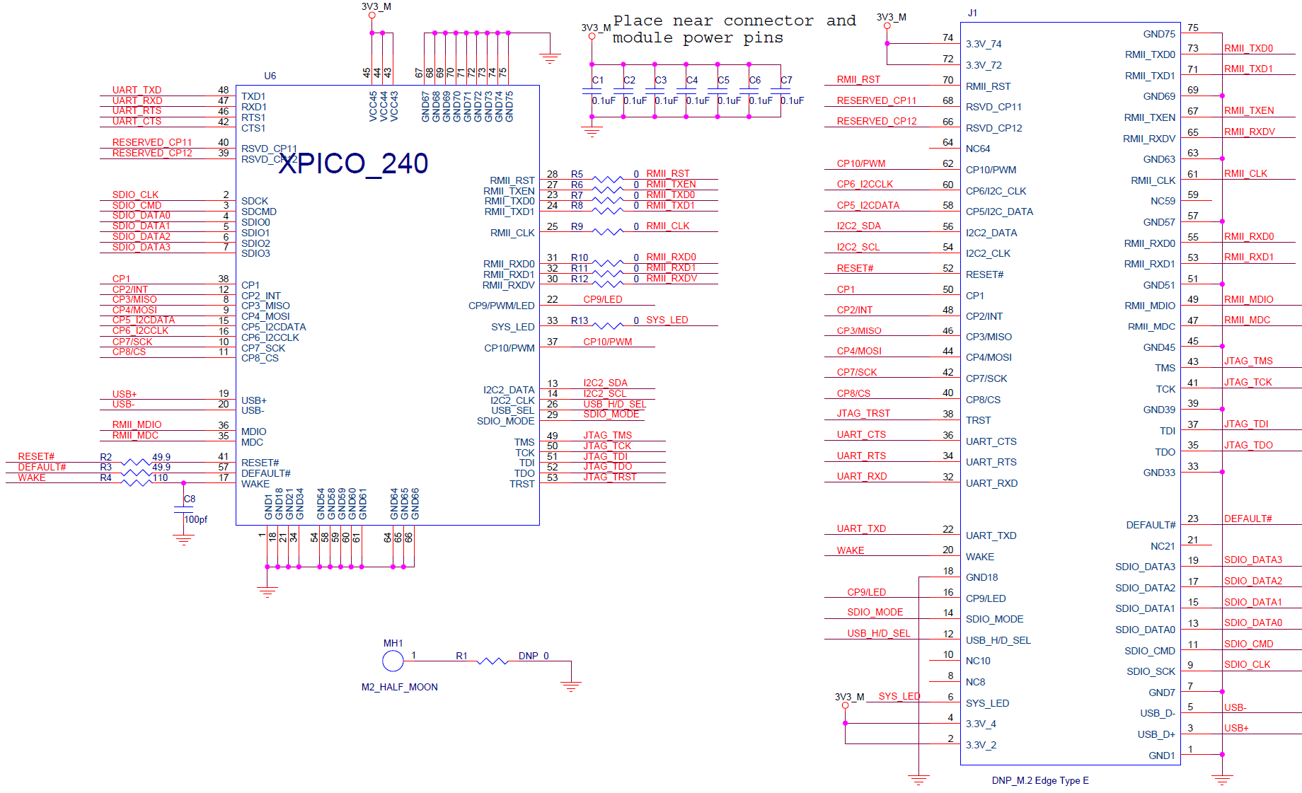
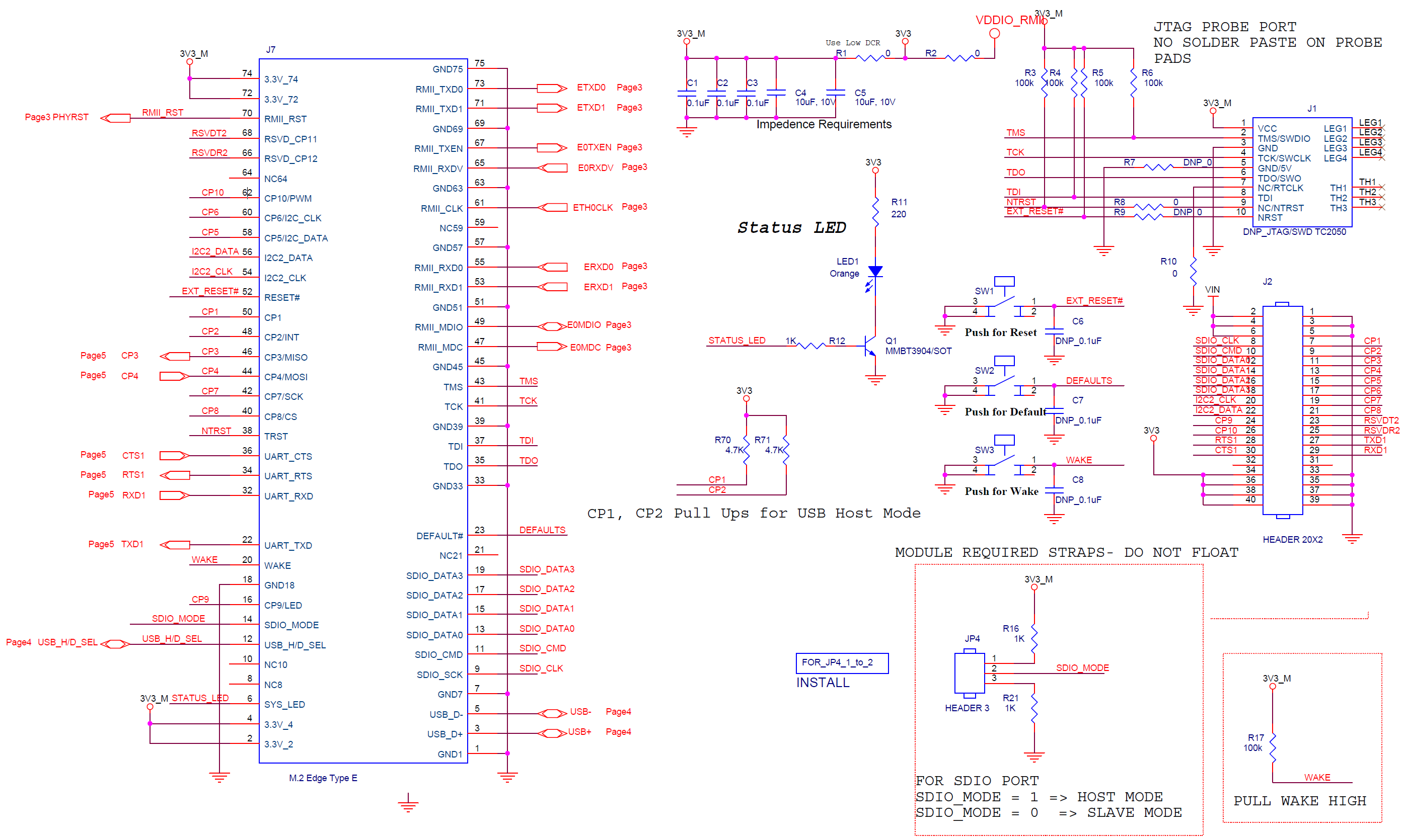
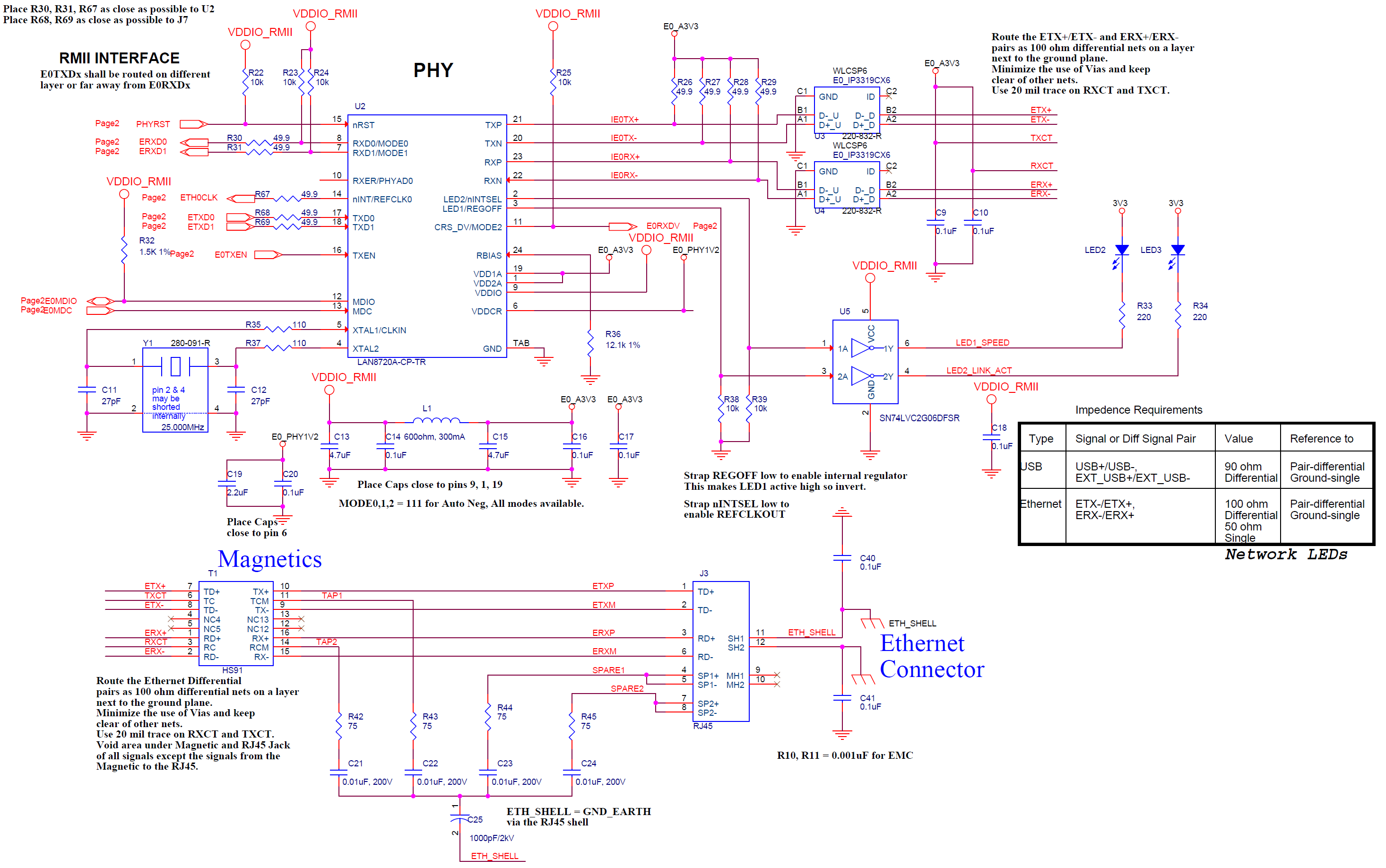
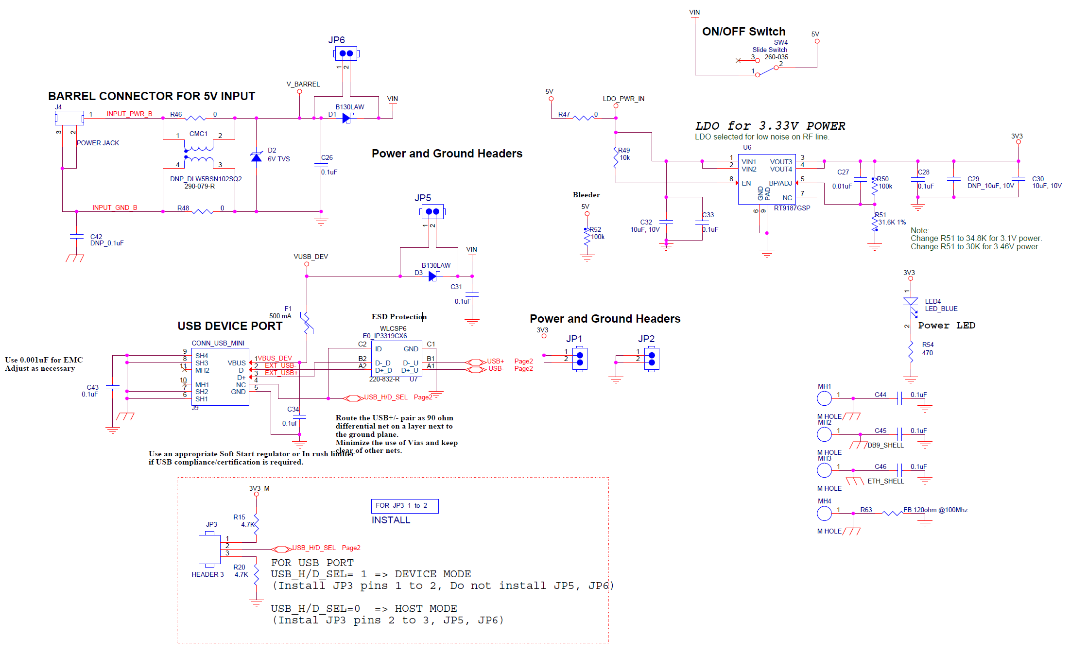
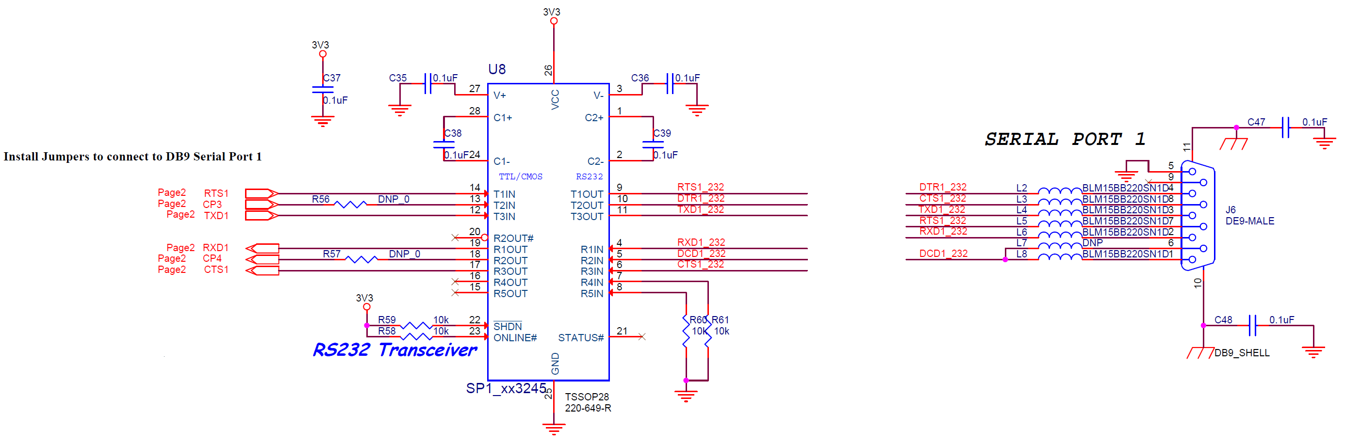
Evaluation Board Schematics