Pin Locations & Descriptions
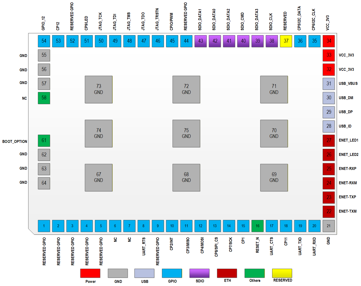
The LGA xPico 600 pin locations are shown below.
Pin Definitions
The pin type abbreviations used in the I/O and Status After Reset columns in the signal description tables in this document are described below.
I/O Parameter Definitions
| Type | Description |
|---|---|
| AIO | Analog Input/Output |
| DI | Digital Input |
| DO | Digital Output |
| DIO | Digital Input/Output |
| PI | Power Input |
| PU | Pull Up |
| HI-Z | High Impedance |
| H | High Level |
xPico 600 Pin and Signal Descriptions
| LGA Pin No. | M.2 Pin No. | Signal |
|---|---|---|
| 1 | N/C | Reserved GPIO |
| 2 | N/C | Reserved GPIO |
| 3 | N/C | Reserved GPIO |
| 4 | N/C | Reserved GPIO |
| 5 | N/C | Reserved GPIO |
| 6 | 46 | N/C |
| 7 | 48 | N/C |
| 8 | 34 | UART_RTS |
| 9 | N/C | Reserved GPIO |
| 10 | 23 | CP2/INT |
| 11 | 50 | CP3/MISO |
| 12 | 56 | CP4/MOSI |
| 13 | 59 | CP8/SPI_CS |
| 14 | 54 | CP7/SCK |
| 15 | 62 | CP1 |
| 16 | 52 | RESET_N |
| 17 | 36 | UART_CTS |
| 18 | 21 | CP11 |
| 19 | 22 | UART_TXD |
| 20 | 32 | UART_RXD |
| 21 | 1 | GND |
| 22 | 73 | ENET-TXM |
| 23 | 71 | ENET-TXP |
| 24 | 67 | ENET-RXM |
| 25 | 65 | ENET-RXP |
| 26 | 49 | ENET_LED2 |
| 27 | 47 | ENET_LED1 |
| 28 | 40 | USB_ID |
| 29 | 3 | USB_DP |
| 30 | 5 | USB_DM |
| 31 | 64 | USB_VBUS |
| 32 | 2 | VCC_3V3 |
| 33 | 4 | VCC_3V3 |
| 34 | 72 | VCC_3V3 |
| 35 | 60 | CP6/I2C_CLK |
| 36 | 58 | CP5/I2C_DATA |
| 37 | N/C | Reserved |
| 38 | 9 | SDIO_CLK |
| 39 | 19 | SDIO_DATA3 |
| 40 | 11 | SDIO_CMD |
| 41 | 17 | SDIO_DATA2 |
| 42 | 13 | SDIO_DATA0 |
| 43 | 15 | SDIO_DATA1 |
| 44 | N/C | Reserved GPIO |
| 45 | 6 | CP10/PWM |
| 46 | 38 | JTAG_TRSTN |
| 47 | 35 | JTAG_TDO |
| 48 | 43 | JTAG_TMS |
| 49 | 37 | JTAG_TDI |
| 50 | 41 | JTAG_TCK |
| 51 | 16 | CP9/LED |
| 52 | N/C | Reserved GPIO |
| 53 | 44 | CP12 |
| 54 | 20 | UART_WAKE |
| 55 | 7 | GND |
| 56 | 18 | GND |
| 57 | 33 | GND |
| 58 | 61 | N/C |
| 61 | 42 | BOOT_OPTION |
| 62 | 39 | GND |
| 63 | 45 | GND |
| 64 | 51 | GND |
| 67 | 57 | GND |
| 68 | 63 | GND |
| 69 | 69 | GND |
| / | 74 | VCC_3V3 |
| 70, 71, 72, 73, 74, 75 | 75 | GND |